
 Home
>
Products
>
SiC Substrate
>
Home
>
Products
>
SiC Substrate
>
|
| Place of Origin | china |
| Brand Name | zmsh |
| Model Number | sic-6inch 4h-n |
| Property | 4H-SiC, Single Crystal | 6H-SiC, Single Crystal |
| Lattice Parameters | a=3.076 Å c=10.053 Å | a=3.073 Å c=15.117 Å |
| Stacking Sequence | ABCB | ABCACB |
| Mohs Hardness | ≈9.2 | ≈9.2 |
| Density | 3.21 g/cm3 | 3.21 g/cm3 |
| Therm. Expansion Coefficient | 4-5×10⁻⁶/K | 4-5×10⁻⁶/K |
| Refraction Index @750nm |
no = 2.61 ne = 2.66 |
no = 2.60 ne = 2.65 |
| Dielectric Constant | c~9.66 | c~9.66 |
| Thermal Conductivity (N-type, 0.02 ohm.cm) |
a~4.2 W/cm·K@298K c~3.7 W/cm·K@298K |
|
| Thermal Conductivity (Semi-insulating) |
a~4.9 W/cm·K@298K c~3.9 W/cm·K@298K |
a~4.6 W/cm·K@298K c~3.2 W/cm·K@298K |
| Band-gap | 3.23 eV | 3.02 eV |
| Break-Down Electrical Field | 3-5×10⁶V/cm | 3-5×10⁶V/cm |
| Saturation Drift Velocity | 2.0×10⁵m/s | 2.0×10⁵m/s |
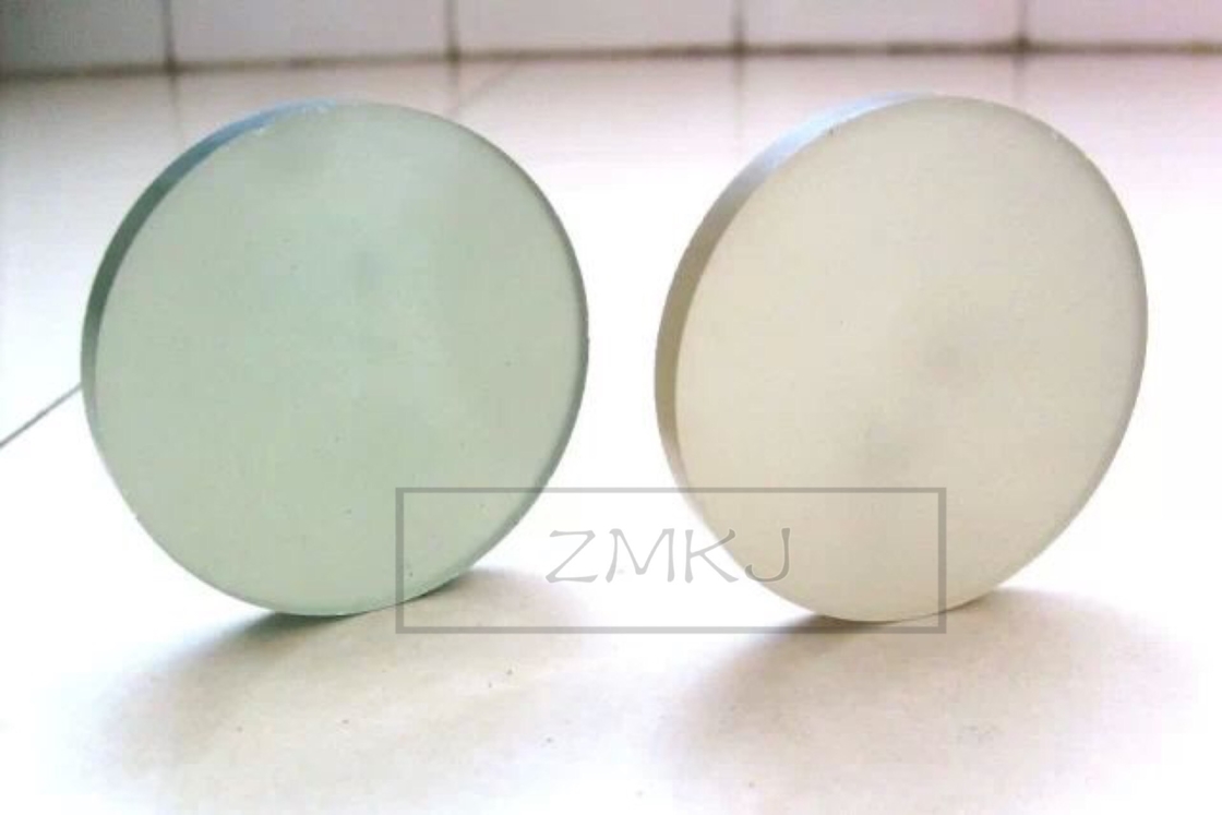
| 6 inch diameter Silicon Carbide (SiC) Substrate Specification |
| Grade | Z grade | P grade | R grade | D grade | |
| ZERO MPD | Production | Research Grade | Dummy Grade | ||
| Diameter | 150mm±0.5 mm | ||||
| Thickness | 350 μm±25μm or 500±25um or by customized size | ||||
| Wafer Orientation | Off axis : 4.0° toward <1120 > ±0.5° for 4H-N | ||||
| Micropipe Density | ≤1cm-2 | ≤5 cm-2 | ≤15 cm-2 | ≤50 cm-2 | |
| Resistivity | 4H-N | 0.015~0.028 Ω·cm | |||
| 4/6H-SI | >1E5 Ω·cm | ||||
| Primary Flat | {10-10}±5.0° | ||||
| Primary Flat Length | 47.5mm±2.5 mm | ||||
| Edge exclusion | 3mm | ||||
| TTV/Bow /Warp | ≤15μm /≤40μm /≤60μm | ||||
| Roughness | Polish Ra≤1 nm | ||||
| CMP Ra≤0.5 nm | |||||
| None | None | 1 allowed, ≤1 mm | |||
| Cracks by high intensity light | |||||
| Hex Plates by high intensity light | Cumulative area≤1 % | Cumulative area≤1 % | Cumulative area≤3 % | ||
| None | Cumulative area≤2 % | Cumulative area≤5% | |||
| Polytype Areas by high intensity light | |||||
| 3 scratches to 1×wafer diameter cumulative length | 5 scratches to 1×wafer diameter cumulative length | 8 scratches to 1×wafer diameter cumulative length | |||
| Scratches by high intensity light | |||||
| Edge chip | None | 3 allowed, ≤0.5 mm each | 5 allowed, ≤1 mm each | ||
| Contamination by high intensity light | None | ||||
FAQ:
Q: What's the way of shipping and cost?
A:(1) We accept DHL, Fedex, EMS etc.
(2) it is fine If you have your own express account ,If not,we could help you ship them and
Freight is in accordance with the actual settlement.
Q: How to pay?
A: T/T 100% deposit before delivery.
Q: What's your MOQ?
A: (1) For inventory, the MOQ is 1pcs. if 2-5pcs it's better.
(2) For customized commen products, the MOQ is 10pcs up.
Q: What's the delivery time?
A: (1) For the standard products
For inventory: the delivery is 5 workdays after you place the order.
For customized products: the delivery is 2 -4 weeks after you order contact.
Q: Do you have standard products?
A: Our standard products in stock. as like substrates 4inch 0.35mm.
Contact Us at Any Time

