
 Home
>
Products
>
Gallium Nitride Wafer
>
Home
>
Products
>
Gallium Nitride Wafer
>
|
| Place of Origin | china |
| Brand Name | zmkj |
| Model Number | customized orientations sapphire |
customized orientation 2inch SSP Sapphire carrier substrate chip for GaN template grow application
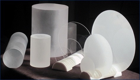
Sapphire wafer carriers are manufactured to exacting specifications and offer a stable carrier for processing GaAs,GaN,AlN and other semiconductors Template. Sapphire wafer carriers are durable, chip, chemical and scratch resistant and will stand up to repeated use. Because of sapphire's extreme hardness, it will provide stronger and more durable carrier than quartz and other materials.
The specification of sapphire We can offer:
Size:Diameters from 2" to 6"
Material:Optical grade High Purity Sapphire
Shape:Custom make hole sizes and patterns Semi Standard Flats and laser marking available
Orientations: C-axis,A-axis,M-axis,R-axis,or other Speical axis as like 1-10°off C-plane±0.1°,
Diameter:2inch 50.8mm,3inch 76.2mm,or bigger
Surface:SSP/ DSP ( by your need)
Thickness: 330um or 430um for 2inch;350um or 500um or 650um for 4inch,
Thickness Tolerace:±10um
Ra: Front side Ra<0.3nm/ back side Lapped Ra0.8~1.2um( or double side polished)
TTV/bow:<10um
Package:25pcs cassette case in 100 grade cleaning rooms
![]()
The templateof GaN AlN We also can offer:
Item GaN-T-N GaN-T-S
Dimensions Ф 2” Dia50.8mm
GaN Thickness 15 μm, 20 μm, 30 μm, 40 μm 30 μm, 90 μm
Orientation C-axis(0001) ± 1°
Conduction Type N-type Semi-Insulating
Resistivity(300K) < 0.05 Ω·cm >106 Ω·cm
Dislocation Density Less than 1x108 cm-2
Substrate structure Thick GaN on 430um or 330um Sapphire(0001)
Useable Surface Area > 90%
Polishing Standard: SSP / Option: DSP
Package Packaged in a class 100 clean room environment, in cassettes of 25pcs
or single wafer containers, under a nitrogen atmosphere.
![]()
![]()
FAQ:
Q: What's the way of shipping and cost?
A:(1) We accept DHL, Fedex, EMS etc.
(2) If you have your own express account, it's great.If not,we could help you ship them.
Freight is in accordance with the actual settlement Or by FOB.
Q: How to pay?
A: T/T,
Q: What's your MOQ?
A: (1) our standard size For inventory, the MOQ is 25pcs in one cassette
(2) For customized products, the MOQ is 25pcs up.
Q: What's the delivery time?
For inventory: the delivery is 5 workdays after you place the order.
For customized products: the delivery is 2 or 4 weeks after you place the order.
Contact Us at Any Time

