
|
| Place of Origin | china |
| Brand Name | zmkj |
| Certification | ROHS |
| Model Number | high purity un-doped 4h-semi |
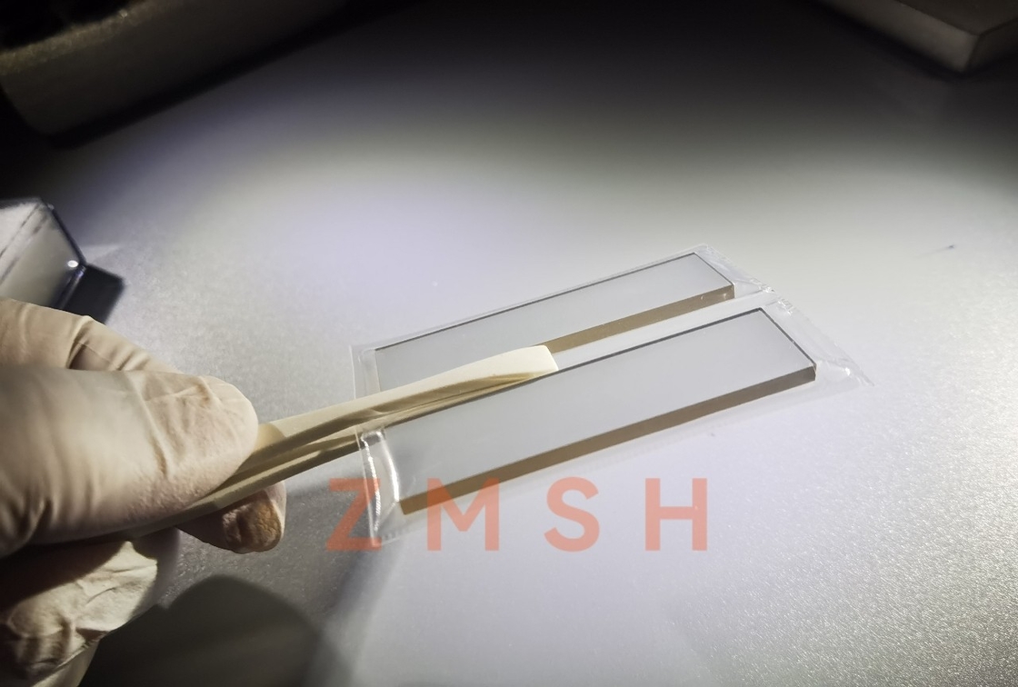
High purity HPSI 4H-SEMI 4H-N 10X10mm 5x5mm sic wafers DSP transparent sic crystal optical lens 4H-SEMI by customzied size
ZMSH offers SiC wafer and Epitaxy: SiC wafer is the third generation wide bandgap semiconductor material with excellent performance. It has the advantages of wide bandgap, high thermal conductivity, high breakdown electric field, high intrinsic temperature, radiation resistance, good chemical stability and high electron saturation drift rate. SiC wafer has also great application prospects in aerospace, rail transit, photovoltaic power generation, power transmission, new energy vehicles and other fields, and will bring revolutionary changes to power electronics technology. Si face or C face is CMP as epi-ready grade, packed by nitrogen gas, each wafer is in one wafer container, under 100 clean class room.
Epi-ready SiC wafers has N type or Semi-insulating, its polytype are 4H or 6H in different quality grades, Micropipe Density (MPD): Free, <5/cm2, <10/cm2, <30/cm2,<100/cm2, and the available size is 2”,3”,4” and 6”.Regarding SiC Epitaxy, its Wafer to wafer thickness uniformity: 2% , and Wafer to wafer doping uniformity: 4%, available doping concentration are from undoped, E15,E16,E18,E18/cm3, n type and p type epi layer are both available, epi defects are below 20/cm2; All the substrate should be used production grade for epi growth;N-type epi layers <20 microns are preceded by n-type, E18 cm-3, 0.5 μm buffer layer; N-type epi layers≥20 microns are preceded by n-type, E18, 1-5 μm buffer layer; N-type doping is determined as an average value across the wafer (17 points) using Hg probe CV; Thickness is determined as an average value across the wafer (9 points) using FTIR.
2. substrates size of our standard size
|
4 inch diameter Silicon Carbide (SiC) Substrate Specification |
|||||||||
| Grade | Zero MPD Grade | Production Grade | Research Grade | Dummy Grade | |||||
| Diameter | 76.2 mm±0.3 mm or 100±0.5mm; | ||||||||
| Thickness | 500±25um | ||||||||
| Wafer Orientation | 0° off (0001)axis | ||||||||
| Micropipe Density | ≤1 cm-2 | ≤5 cm-2 | ≤15 cm-2 | ≤50 cm-2 | |||||
| Resistivity | 4H-N | 0.015~0.028 Ω•cm | |||||||
| 6H-N | 0.02~0.1 Ω•cm | ||||||||
| 4/6H-SI | ≥1E7 Ω·cm | ||||||||
| Primary Flat and length | {10-10}±5.0° ,32.5 mm±2.0 mm | ||||||||
| Secondary Flat Length | 18.0mm±2.0 mm | ||||||||
| Secondary Flat Orientation | Silicon face up: 90° CW. from Prime flat ±5.0° | ||||||||
| Edge exclusion | 3 mm | ||||||||
| TTV/Bow /Warp | ≤15μm /≤25μm /≤40μm | ||||||||
| Roughness | Polish Ra≤1 nm ,CMP Ra≤0.5 nm | ||||||||
| Cracks by high intensity light | None | 1 allowed, ≤2 mm | Cumulative length ≤ 10mm, single length≤2mm | ||||||
| Hex Plates by high intensity light | Cumulative area ≤1% | Cumulative area ≤1% | Cumulative area ≤3% | ||||||
| Polytype Areas by high intensity light | None | Cumulative area ≤2% | Cumulative area ≤5% | ||||||
Sic wafer & ingots 2-6inch and other customized size also can be provided.
3.Products detail display
![]()
![]()
Delivery & Package
Contact Us at Any Time


