
|
| Place of Origin | CHINA |
| Brand Name | zmkj |
| Model Number | LT-001 |
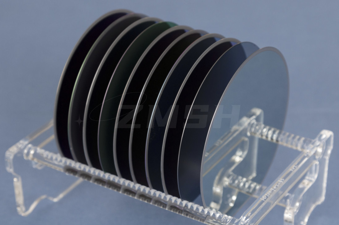
4inch 100mm LT LN thin film For SAW Device for Electronic device
Specification
|
Orientation |
36°Y-cut±0.2° | 42°Y-cut±0.2° | X-cut±0.2° | |
| Diameter | 100±0.3mm , | |||
| 1st OF Flat | 32±2mmperpendicular to X-axis±0.2° | 32±2mm, perpendicular to 112°Y±0.2° | ||
| 2st OF Flat | 10±2mm CW270°from 1st OF | 10±2mm CW315°from 1st OF | 10±2mm CW315° Or 270°from 1st OF | |
| Thickness | 200~250±25um,300-350±25um,500±25um or by customized | |||
| Front surface | "+",Ra<1nm, | |||
| Back surface | GC#1000, GC#2000 Lapped | |||
| LTV | <1um,at5x5mm zone | |||
| BOW | ≤25um | |||
Product display
![]()
![]()
![]()
FAQ
Q. Do you have any stock of wafer or ingots?
yes,aslike 3inch,4inch commen size substrates wafers are in stocks.
Q. Where is your company located?
Our company located in shanghai,China. factory is in wuxi city.
Q. How long will take to get the products?
Generally it will take 1~4 weeks to process and then delivery.
It is depend on the quantity and the size of the products.
Q: How about pay term & delivery ?
T/T 50%deposit and left part before delivery by FOB .
Contact Us at Any Time


