
 Home
>
Products
>
GaAs Wafer
>
Home
>
Products
>
GaAs Wafer
>
|
| Place of Origin | china |
| Brand Name | zmsh |
| Certification | ROHS |
| Model Number | 6INCH GaAs wafer |
2inch GaAs Substrates Single Crystal Gallium Arsenide Substrates Semi-Conducting N Type
------------------------------------------------------------------------------------------------------------------------------
GaAs wafer
Gallium arsenide (GaAs) is an excellent semiconducting material. It has large direct band gap, high electron mobility, high frequency low noise and high conversion efficiency) and other outstanding advantages.
GaAs substrate is divided into conductive and semi-insulating, widely used in laser (LD), semiconductor light-emitting diode (LED), near infrared laser, quantum well high-power laser and high efficiency solar panels; HEMT and HBT chips for radar, microwave, millimeter wave or ultra-high speed computers and optical communications; Radio frequency devices for wireless communication, 4G, 5G, satellite communication, WLAN.
Recently, gallium arsenide substrate has also made great progress in mini-LED, Micro-LED and red light LED, which is widely used in AR/VR wearable devices.
GaAs Wafer Market&Application
Gallium arsenide is an important semiconductor materialIt belongs to gro up lll-V compound semiconductors and the zincblende crystal lattice structure, with a lattice constantof5.65x10-10ma melting point of1237° C,and a band gap of 1.4 electron volts.Gallium arsenide can be made into semi-insulating high-resistance materialswhich can be used to make integrated circuit substratesinfrared detectorsgamma photon
detectors,etc.Because its electron mobility is 5to6times greater than sili con,SI GaAs substrate has been importantly used in the fabrication of microwave devices and high-speed digital circuits.Semiconductor devices fabricated on gallium arsenide have the advantages of high frequency high temperature, lowtemperature performancelow noiseand strong rac iation resistance,which make the GaAs substrate market enlarge.
|
GaAs (Gallium Arsenide) ,Semi-insulating for Microelectronics Applications
|
||
|
Item
|
Specifications
|
Remarks
|
|
Conduction Type
|
Insulating
|
|
|
Growth Method
|
VGF
|
|
|
Dopant
|
Undoped
|
|
|
Wafer Diamter
|
2, 3, 4 & 6 inch
|
Ingot available
|
|
Crystal Orientation
|
(100)+/- 0.5°
|
|
|
OF
|
EJ, US or notch
|
|
|
Carrier Concentration
|
n/a
|
|
|
Resistivity at RT
|
>1E7 Ohm.cm
|
|
|
Mobility
|
>5000 cm2/V.sec
|
|
|
Etch Pit Density
|
<8000 /cm2
|
|
|
Laser Marking
|
upon request
|
|
|
Surface Finish
|
P/P
|
|
|
Thickness
|
350~675um
|
|
|
Epitaxy Ready
|
Yes
|
|
|
Package
|
Single wafer container or cassette
|
|
packing
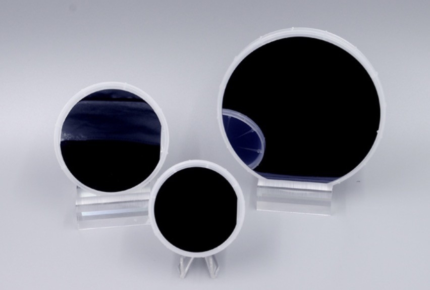
![]()
![]()
![]()
ABOUT OUR ZMKJ
Q: What's the MOQ?
(1) For inventory, the MOQ is 5pcs.
(2) For customized products, the MOQ is 10pcs-30pcs.
Q: Do you have inspection report for material?
We can supply detail report for our products.
Contact Us at Any Time

