Send Message
SHANGHAI FAMOUS TRADE CO.,LTD
Mail: eric_wang@zmsh-materials.com TEL: 86-1580-1942596
Home > Products > Gallium Nitride Wafer >
Transparent 10x15mm 001 Orientation Gallium Oxide GaO Substrate For LEDs Application
  • Transparent 10x15mm 001 Orientation Gallium Oxide GaO Substrate For LEDs Application
  • Transparent 10x15mm 001 Orientation Gallium Oxide GaO Substrate For LEDs Application

Transparent 10x15mm 001 Orientation Gallium Oxide GaO Substrate For LEDs Application

Place of Origin china
Brand Name zmsh
Certification ROHS
Model Number GaO substrates
Product Details
Application:
UV Light-emitting Diodes (LEDs)
Size:
Customized
Surface:
Cmp/etched
Doped:
Mg-doped
MOQ:
10PCS
Grade:
Research Grade/dummy Grade
High Light: 

LEDs Gallium Nitride Wafer

,

Transparent Gallium Oxide GaAS Substrate

,

Gallium Oxide Substrate 10x15mm

Product Description

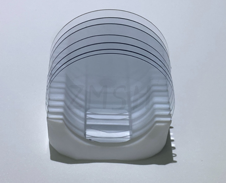
10x15mm 001 Gallium oxide GaO substrate Mg doping
 
10x10mm Gallium oxide substrate monocline structure
------------------------------------------------------------------------------------------------------------------------------

Specification detail
 
Orientation100100100
DopingUIDMgFe
electrical parameter
1×10¹⁷~3×1018cm-3
≥1010Ω·cm≥1010Ω·cm
arcsec
≤150≤150≤150
dislocation density<1×105 cm-2<1×105 cm-2<1×105 cm-2


Feature

Although gallium oxide has poor thermal conductivity, its band gap exceeds that of silicon carbide, gallium nitride and silicon. Since the band-gap width measures the energy required to bring electrons into the on-state, systems made of materials with a wider band-gap can be thinner and lighter than those made of materials with a narrower band-gap, and can handle higher power, promising high-voltage and low-loss power components at low cost. In addition, the wide band gap allows operation at higher temperatures, reducing the need for a large cooling system.


Application

Gallium oxide is a new kind of power semiconductor material, which has more and more obvious advantages in high power applications. Experts generally believe that gallium oxide will become an important supplement to silicon carbide and gallium nitride.
Gallium oxide is more likely to play a role in expanding the power and voltage range available for ultra-wide bandgap systems. The most promising applications may be high-voltage rectifiers in power regulation and distribution systems, such as electric vehicles and photovoltaic solar systems.


ABOUT OUR ZMKJ

     ZMKJ locates in the city of Shanghai, Which is the best city of China, and our factory is founded
in Wuxi city in 2014.We specialize in processing a varity of materials into wafers, substrates
and custiomized optical glass parts.components widely used in electronics, optics,
optoelectronics and many other fields. We also have been working closely with many domestic
and oversea universities, research institutions and companies, provide customized products
and services for their R&D projects.


Related products:GaAs wafer
Transparent 10x15mm 001 Orientation Gallium Oxide GaO Substrate For LEDs Application 0Transparent 10x15mm 001 Orientation Gallium Oxide GaO Substrate For LEDs Application 1
 
 
Packaging – Logistcs
Worldhawk concerns each details of the package , cleaning, anti-static , shock treatment .
According to the quantity and shape of the product , we will take a different packaging process!
 
FAQ –
Q: What you can supply logistics and cost?
(1) We accept DHL, Fedex, TNT, UPS, EMS, SF and  by FOB
 and pay condition of 50% deposit,50% before delivery.
 
Q: What's the delivery time?
For inventory: the delivery is 5 workdays after order.
For customized products: the delivery is 2 or 3 workweeks after order.
 

Q: What's the MOQ?
(1) For inventory, the MOQ is 5pcs.
(2) For customized products, the MOQ is 10pcs-30pcs.
Q: Do you have inspection report for material?
We can supply detail report for our products.


Contact Us at Any Time

86-1580-1942596
Rm5-616,No.851,Dianshanhu avenue, Qingpu area,Shanghai city,CHINA
Send your inquiry directly to us