Indium Phosphide Wafer InP Semiconductor Substrates Epitaxial 2'' 3'' Thickness 350um
Description of Indium Phosphide:
Indium Phosphide (InP) chips are a widely used material in optoelectronics and semiconductor devices. It has the following advantages:
- High electron mobility: Indium phosphide chips have a high electron mobility, which means that electrons move faster through the material.
- Controlled material properties: The properties of indium phosphide wafers can be regulated by controlling the epitaxial growth process of the material and doping techniques.
- Wide band gap: The indium phosphide wafer has a wide band gap, enabling it to operate in the visible and infrared light ranges.
- High saturation drift speed: The indium phosphide wafer has a high saturation drift speed, which means that the electron drift speed reaches the maximum under a high electric field.
- Excellent thermal conductivity: The indium phosphide wafer has a high thermal conductivity, which means that it is able to efficiently conduct and dissipate heat, thereby improving the reliability and performance stability of the device.
Features of Indium Phosphide:
Indium Phosphide (InP) chips have some remarkable characteristics that make them widely used in optoelectronics and semiconductors. The following are some of the main characteristics of indium phosphide chip materials:
- Direct band gap: Indium phosphide has a direct band gap characteristic that makes it excellent in optical devices.
- Wide band gap range: Indium phosphide has a wide band gap ranging from infrared to ultraviolet spectrum.
- High electron mobility: Indium phosphide has a high electron mobility, which makes it excellent in high-frequency electronics and high-speed optoelectronics.
- Excellent thermal conductivity: Indium phosphide has a high thermal conductivity and can effectively dissipate heat.
- Good mechanical and chemical stability: Indium phosphide chips have good mechanical and chemical stability and can maintain stability and reliability under different environmental conditions.
- Adjustable band structure: The band structure of indium phosphide materials can be regulated by doping and alloying techniques to meet the requirements of different devices.
Technical Parameters of Indium Phosphide:
|
Item
|
Parameter
|
UOM
|
|
Material
|
InP
|
|
|
Conduction type/Dopant
|
S-C-N/S
|
|
|
Grade
|
Dummy
|
|
|
Diameter
|
100.0+/-0.3
|
mm
|
|
Orientation
|
(100) +/-0.5°
|
|
|
Lamellar twin area
|
useful single crystal area with (100) orienation > 80%
|
|
|
Primary Flat Orientation
|
EJ(0-1-1)
|
mm
|
|
Primary Flat Length
|
32.5+/-1
|
|
|
Secondary Flat Orientation
|
EJ(0-11)
|
|
|
Secondary Flat Length
|
18+/-1
|
|
Applications of Indium Phosphide:
Indium Phosphide (InP) wafers have a wide range of applications in optoelectronics and semiconductor substrates:
- Optical communication: InP wafers are widely used in the field of optical communication for high-speed optical fiber communication systems. They are used to fabricate devices such as lasers, optical modulators, optical receivers, optical amplifiers and optical fiber couplers.
- Photoelectronic devices: InP wafers are used to make photoelectronic devices such as photodiodes, photodetectors, solar cells and photocouplers.
- High-speed electronic devices: InP substrates are widely used in the field of high-frequency electronic devices. In particular, InP wafes' high electron mobility transistors (HEMTs) are used to prepare devices such as high-frequency amplifiers, RF switches and microwave integrated circuits for applications such as wireless communications, radar systems and satellite communications.
- Integrated optical devices: InP wafers are used to prepare integrated optical devices such as optical waveguides, optical modulators, optical switches and optical amplifiers.
- Photonics research: InP wafers play an important role in photonics research. They are used in laboratory research, quantum optics, quantum information processing and optical quantum devices.
- In addition to the above applications, InP wafers are also used in other fields, such as optical sensing, biomedicine, light storage and semiconductor substrates

FAQ:
Q1: What brand name is the InP wafer?
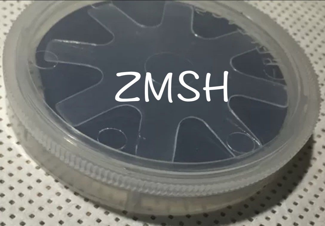
A1: The InP wafer is made by ZMSH.
Q2: What's the diameter of the InP wafer?
A2: The diameter of InP wafer is 2'', 3'', 4''.
Q3: Where is the InP wafer from?
A3: The InP wafer is from China.
Q4: Is the InP wafer ROHS certified?
A4: Yes, the InP wafer is ROHS certified.
Q5: How many InP wafes can I buy at 1 time?
A5: The minimum order quantity of the InP wafer is 5pcs.
Other products:
Silicon wafers

 Home
>
Products
>
Indium Phosphide Wafer
>
Home
>
Products
>
Indium Phosphide Wafer
>