
 Home
>
Products
>
SiC Substrate
>
Home
>
Products
>
SiC Substrate
>
|
| Place of Origin | CHINA |
| Brand Name | SICC |
| Certification | CE |
| Model Number | 4h-n |
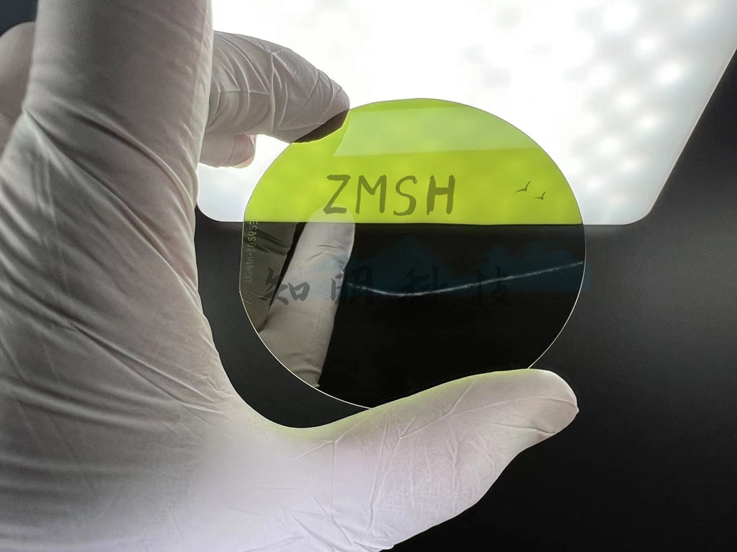
2inch dia50.8mm 330μm thickness 4H-N Type SiC substrate Production Grade
2inch Silicon Carbide Wafers 6H or 4H N-type or Semi-Insulating SiC Substrates
4H-N Type / Semi Insulating SiC Substrates 2inch 3inch 6inch Silicon Carbide Wafers
what is SiC subatrate
A SiC substrate refers to a wafer made of silicon carbide (SiC), which is a wide-bandgap semiconductor material that has excellent electrical and thermal properties. SiC substrates are commonly used as a platform for the growth of epitaxial layers of SiC or other materials, which can be used to fabricate various electronic and optoelectronic devices, such as high-power transistors, Schottky diodes, UV photodetectors, and LEDs.
SiC substrates are preferred over other semiconductor materials, such as silicon, for high-power and high-temperature electronics applications due to their superior properties, including higher breakdown voltage, higher thermal conductivity, and higher maximum operating temperature. SiC devices can operate at much higher temperatures than silicon-based devices, making them suitable for use in extreme environments, such as in automotive, aerospace, and energy applications.
Applications
III-V Nitride Deposition
Optoelectronic Devices
High-Power Devices
High-Temperature Devices
High-Frequency Power Devices
Specification
| Grade | Production Grade | Research Grade | Dummy Grade | |
| Diameter | 50.8 mm +/- 0.38 mm | |||
| Thickness |
N-type 330 um +/- 25 um Semi-Insulating 250 um +/- 25 um |
|||
| Wafer Orientation |
On axis: <0001> +/- 0.5 deg for 6H-N /4H-N /4H-SI /6H-SI Off axis: 4.0 deg toward <11-20> +/-0.5 deg for 4H-N /4H-SI |
|||
| Micropipe Density (MPD) | 5 cm-2 | 15 cm-2 | 30 cm-2 | |
|
Electrical Resistivity (Ohm-cm) |
4H-N | 0.015~0.028 | ||
| 6H-N | 0.02~0.1 | |||
| 4/6H-SI | >1E5 | (90%) >1E5 | ||
| Doping Concentration |
N-type: ~ 1E18/cm3 SI-type (V-doped): ~ 5E18/cm3 |
|||
| Primary Flat | {10-10} +/- 5.0 deg | |||
| Primary Flat Length | 15.9 mm +/- 1.7 mm | |||
| Secondary Flat Length | 8.0 mm +/- 1.7 mm | |||
| Secondary Flat Orientation | Silicon face up: 90 deg CW from Prime flat +/- 5.0 deg | |||
| Edge exclusion | 1 mm | |||
| TTV / Bow / Warp | 15 um / 25um / 25um | |||
| Surface Roughness | Optical Polish Ra 1 nm on the C face | |||
| CMP Ra 0.5 nm on the Si face | ||||
| Cracks inspected by high intensity light | None | None | 1 allowed, 1 mm | |
| Hex Plates inspected by high intensity light* | Cumulative area 1 % | Cumulative area 1 % | Cumulative area 3 % | |
| Polytype Areas inspected by high intensity light* | None | Cumulative area 2 % | Cumulative area 5% | |
| Scratches inspected by high intensity light** |
3 scratches to 1wafer diameter cumulative length |
5 scratches to 1 wafer diameter cumulative length |
8 scratches to 1 wafer diameter cumulative length |
|
| Edge chipping | None | 3 allowed, 0.5 mm each | 5 allowed, 1 mm each | |
| Surface contamination as inspected by high intensity light | None | |||
![]()
![]()
Industrial chain
The silicon carbide SiC industrial chain is divided into substrate material preparation, epitaxial layer growth, device manufacturing and downstream applications. Silicon carbide monocrystals are usually prepared by physical vapor transmission (PVT method), and then epitaxial sheets are generated by chemical vapor deposition (CVD method) on the substrate, and the relevant devices are finally made. In the industrial chain of SiC devices, due to the difficulty of substrate manufacturing technology, the value of the industrial chain is mainly concentrated in the upstream substrate link.
ZMSH company provides provides 100mm and 150mm SiC wafers. With its hardness (SiC is the second hardest material in the world) and stability under heat and high voltage current, this material is being widely used in several industries.
Price
ZMSH company offers the best price on the market for high quality SiC wafers and SiC crystal substrates up to six (6) inch diameter. Our price matching policy guarantees you the best price for the SiC crystal products with comparable specifications. CONTACT US today to get your quote.
Customization
Customized SiC crystal products can be made to meet customer's particular requirements and specifications.
Epi-wafers can also be custom made upon request.
FAQ
Q: What's the wayof shipping and cost and pay term ?
A:(1) We accept 50% T/T In advance and left 50% before delivery by DHL, Fedex, EMS etc.
(2) If you have your own express account, it's great.If not,we could help you ship them.
Freight is in accordance with the actual settlement.
Q: What's your MOQ?
A: (1) For inventory, the MOQ is 3pcs.
(2) For customized products, the MOQ is 10pcs up.
Q: Can I customize the products based on my need?
A: Yes, we can customize the material, specifications and shape, size based on your needs.
Q: What's the delivery time?
A: (1) For the standard products
For inventory: the delivery is 5 workdays after you place the order.
For customized products: the delivery is 2 or 3 weeks after you place the order.
(2) For the special-shaped products, the delivery is 4 workweeks after you place the order.
Contact Us at Any Time

