logo
Good price  online

products details

Created with Pixso. Home Created with Pixso. Products Created with Pixso.
SiC Substrate
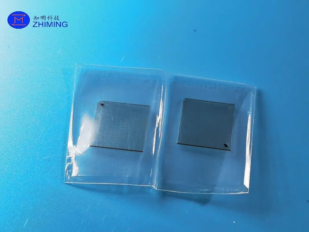
Created with Pixso. Sic Wafer HPSI:High-purity semi-insulating High thermal conductivity MPD controllable

Sic Wafer HPSI:High-purity semi-insulating High thermal conductivity MPD controllable

Brand Name: ZMSH
Model Number: Sic Wafer HPSI
MOQ: 25
Price: Fluctuates with market
Delivery Time: 2-4 weeks
Payment Terms: T/T
Detail Information
Place of Origin:
SHANGHAI,CHINA
Polytype:
Mainstream 4H-SiC
Diameter:
4/6/8 Inch Available
Thickness:
Standard Sizes Are 350μm, 500μm, And 650μm
Resistivity:
≥1×10¹⁰ Ω・cm (HPSI Core Electrical Specification)
Surface Treatment:
Single-sided/double-sided CMP Mirror Polishing
Micropipe Density:
Mass Production Grade ≤1 Ea/cm²
Product Description

Information of HPSI SiC Wafers

    HPSI (High Purity Semi-Insulating) silicon carbide wafers are critical foundational substrates for high-frequency GaN RF devices and advanced third-generation semiconductors. With the rapid expansion of 5G communication, millimeter-wave radar and aerospace electronics markets, the global SiC substrate market is projected to exceed USD 2 billion by 2030, playing an irreplaceable strategic role in next-generation wireless communication and high-power electronic systems.Sic Wafer HPSI:High-purity semi-insulating High thermal conductivity MPD controllable


    Upstream: High-purity silicon carbide powder (above 6N grade), physical vapor transport (PVT) crystal growth furnaces, and high-purity graphite thermal field components. High-end crystal growth equipment and ultra-high-purity raw materials still face partial import dependence in the industrial chain. Midstream: SiC single crystal growth → ingot shaping → multi-wire slicing → lapping → chemical mechanical polishing (CMP) → epitaxy-ready surface treatment. This segment features extremely high technical barriers, with crystal yield and defect control as core competitive indicators. Downstream: GaN RF power devices (accounting for the largest share of HPSI SiC consumption), 5G base station power amplifiers, millimeter-wave radar chips, aerospace electronic components, high-frequency microwave devices, and high-voltage power device prototypes. Downstream demand continues to grow driven by communication technology upgrading and new energy and defense industries.


    4H HPSI SiC wafers are high-purity semi-insulating single-crystal silicon carbide substrates with <0001> crystal orientation, produced mainly via the Physical Vapor Transport (PVT) crystal growth method. The semi-insulating property is achieved through ultra-high purity control and vanadium doping technology, achieving extremely high resistivity. The epi-ready surface undergoes precision CMP polishing to achieve atomic-level smoothness, meeting strict MOCVD GaN epitaxy requirements.

Key Features

High-Purity Semi-Insulating SiC Material

    Our HPSI SiC wafers are fabricated from 6N-grade high-purity single-crystal silicon carbide (4H-SiC), specially developed for high-frequency RF and high-end semiconductor manufacturing environments. The material features outstanding thermal conductivity, ultra-high electrical resistivity, excellent chemical corrosion resistance and superior mechanical strength, maintaining stable electrical and physical performance under high-temperature epitaxy, high-power operation and harsh plasma processing conditions.

Multiple Polytype & Orientation Options for Diverse Devices

    SiC substrates are available in mainstream polytypes and crystal orientations to match different semiconductor device requirements. 4H-SiC is the dominant choice for RF and power devices with balanced electron mobility and material stability; 6H-SiC options cater to special optoelectronic and high-temperature device scenarios. Custom off-angle specifications (e.g., 4° off-axis) are available to optimize epitaxial layer quality and device yield.

Ultra-Precision CMP Polishing & Flatness Performance

    Available in SSP (Single Side Polished) and DSP (Double Side Polished) grades to fit different process scenarios. Epi-ready CMP polished surfaces achieve ultra-low surface roughness Ra < 0.1 nm, with strictly controlled TTV, BOW and WARP values. The atomic-level smooth, defect-free surface perfectly meets MOCVD GaN epitaxy growth standards, ensuring uniform epitaxial layer deposition and high consistency of device RF performance.Sic Wafer HPSI:High-purity semi-insulating High thermal conductivity MPD controllable

Excellent Electrical & Thermal Properties

    HPSI SiC substrates provide ultra-high resistivity (≥ 1×10¹⁰ Ω·cm) and ultra-low dielectric loss, effectively eliminating signal crosstalk and leakage for high-frequency and high-power RF devices. With thermal conductivity 3–4 times higher than sapphire, they deliver excellent heat dissipation capability, significantly improving device power density and long-term reliability under high-load operation.

Customized Precision Substrate Manufacturing

    Substrate specifications can be fully customized according to customer technical requirements, including:

  • Wafer diameter: 2 / 4 / 6 / 8 inch
  • Standard & customized thickness
  • Crystal polytype & precise off-angle
  • SSP / DSP polishing modes
  • Surface roughness & flatness tolerance
  • Edge chamfer & edge finishing
  • Primary flat / notch positioning design
  • Cleanliness grade & precision cleaning process

Functional Processing & Custom Value-Added Services

    In addition to standard bare SiC wafers, we provide full-process customized functional processing to support diversified customer applications. Available services include:

  • Epitaxial layer growth (GaN / AlGaN on SiC)
  • Full / localized metallization (Ti / Ni / Au / Cr coating)
  • Ultra-thin wafer thinning & stress relief processing
  • High-precision dicing, drilling and special shaping
  • Custom surface finishing (polishing / lapping / etching)
  • Strict quality inspection and complete COA certification

Custom Replacement & OEM-Grade Substrate Solutions

    We support customized SiC wafer development and production based on customer drawings, sample benchmarks, equipment process parameters, existing component specifications and reverse-engineering demands. All products comply with RoHS and REACH standards, providing stable, high-yield substrate solutions for semiconductor process upgrading, equipment matching and localized replacement projects.

Typical Applications

    HPSI SiC wafers are core foundational substrates widely adopted in RF communication and advanced semiconductor industries, applicable for the following devices and manufacturing processes:

  • GaN-based RF power amplifiers and HEMT device manufacturing
  • 5G / 6G base station RF front-end chips
  • Millimeter-wave radar and automotive radar chips
  • Satellite communication and aerospace electronic components
  • Microwave and millimeter-wave monolithic integrated circuits (MMIC)
  • High-frequency power electronic device R&D and prototyping
  • Defense electronics and phased array radar systems
  • High-temperature resistant semiconductor device packaging
  • Semiconductor vacuum equipment and high-temperature insulation parts
  • High-power RF device packaging and thermal management substrates

    HPSI SiC substrates have been commercially mass-produced for mainstream RF and high-end semiconductor scenarios, featuring stable batch consistency, low defect rate and excellent process compatibility.

Product Specifications


Item Specification
Product HPSI Silicon Carbide Wafer / SiC Substrate
Material High Purity Semi-Insulating 4H-SiC Single Crystal
Growth Method Physical Vapor Transport (PVT)
Crystal Structure Hexagonal Wurtzite Structure
Diameter 2" / 4" / 6" / 8" or Customized
Thickness Customized (e.g., 350 µm – 650 µm)
Orientation (0001) C-plane, 4° off-axis / Customized
Surface Finish SSP (Single Side Polished) / DSP (Double Side Polished) / Lapped
Surface Quality Scratch-Dig per MIL-PRF-13830B (e.g., 20/10, 10/5)
Resistivity ≥ 1×10¹⁰ Ω·cm (Semi-Insulating)
Micropipe Density (MPD) ≤ 1 ea/cm² (Production Grade) / Customized
TTV (Total Thickness Variation) ≤ 3 µm (or per customer requirement)
Bow / Warp ≤ 10 µm (or per customer requirement)
Roughness (Ra) Polished: ≤ 0.1 nm / Lapped: ≤ 0.5 µm
Edge Type With Primary Flat / Notch (per SEMI standard)
Edge Profile Chamfered / Rounded as Required
Dopant Vanadium-doped / Intrinsic Semi-Insulating
Purity ≥ 99.9999% (6N Grade)
Coating Uncoated / Epitaxial Layer / Metal Coating Available
Application RF Communication / GaN Epitaxy / Microwave / Aerospace

Why Choose HPSI SiC Wafers for Semiconductor & RF Applications?

    HPSI silicon carbide wafers are core foundational substrates widely applied in GaN RF epitaxy, high-frequency device manufacturing and microwave electronic systems. Serving as the carrier for GaN, AlGaN and other epitaxial layer growth, they operate in extreme manufacturing environments featuring high temperature, high power density, strong plasma erosion and high-frequency electromagnetic fields.

Compared with traditional sapphire, silicon and common ceramic substrate materials, high-purity semi-insulating SiC substrates integrate superior comprehensive physical and electrical properties, making them irreplaceable for high-end RF and high-power semiconductor processes. Key advantages include:Sic Wafer HPSI:High-purity semi-insulating High thermal conductivity MPD controllable

  • Ultra-high thermal conductivity: With thermal conductivity up to 490 W/m·K, 3–4 times higher than sapphire and 10 times higher than silicon, it efficiently dissipates heat generated by high-power devices, greatly improving device power density and service life.
  • Extreme high-temperature stability: Boasting a melting point up to 2700°C, it maintains stable crystal structure and dimensional accuracy under long-term high-temperature epitaxy and high-power operation, effectively avoiding substrate deformation and device performance degradation.
  • Ultra-high semi-insulating performance: Featuring resistivity above 1×10¹⁰ Ω·cm and ultra-low dielectric loss, it provides reliable electrical isolation for high-frequency RF devices, effectively reducing signal crosstalk and insertion loss.
  • Superior chemical inertness: It is resistant to corrosion by various acidic, alkaline and reactive process gases used in semiconductor manufacturing, with no chemical reaction or surface deterioration, ensuring ultra-clean process conditions.
  • Excellent plasma and radiation resistance: It withstands long-term plasma bombardment and high-energy radiation in thin-film deposition and etching processes, with low surface damage rate and stable performance.
  • High mechanical strength and hardness: With Mohs hardness of 9.5, second only to diamond, it delivers excellent wear resistance and structural stability, resisting mechanical damage and warpage during precision processing and thin-film growth.
  • Long-term process durability: It maintains consistent surface flatness and crystal quality in repetitive and rigorous semiconductor production processes, greatly reducing substrate replacement frequency and production costs.

    For the above reasons, HPSI SiC substrates have become the preferred mainstream material for GaN RF devices, millimeter-wave communication chips, aerospace electronics and other core semiconductor components.

Custom SiC Wafer Manufacturing

    We specialize in customized and standardized HPSI SiC wafer manufacturing for RF communication and advanced semiconductor equipment, focusing on high-precision tailored solutions for industrial production and laboratory R&D. We break the limitations of fixed standard specifications and customize wafers fully in accordance with customers’ actual process parameters, equipment matching requirements and device design standards.

    Comprehensive customization options cover full-process wafer parameters and supporting structures:

SiC Wafer Core Parameters

  • Wafer diameter (2/4/6/8 inches and special custom sizes)
  • Wafer thickness
  • Crystal polytype (4H-SiC, 6H-SiC) and off-angle specification
  • Edge shape and chamfering specifications
  • Flat / Notch positioning design
  • Surface roughness and flatness
  • Double-sided / single-sided polishing requirements
  • Ultra-clean surface treatment and stress relief processing

Matching Structural Components

  • Substrate carrier fixture size customization
  • Positioning hole and groove processing
  • Metal matching base and sleeve structure
  • Mounting and fixing interface specifications
  • Integrated assembly of substrate and auxiliary parts

    We can provide finished integrated components assembled with SiC wafers and matching metal/ceramic parts to meet customers’ direct installation and use needs.

    Replacement & Reverse Engineering ServiceSic Wafer HPSI:High-purity semi-insulating High thermal conductivity MPD controllable

    For discontinued SiC wafers, hard-to-source original parts, and non-standard customized substrates for special semiconductor equipment, we provide professional reverse engineering and replacement manufacturing services. Customers can provide the following information for evaluation and quotation:

  • Original equipment part number
  • Detailed technical drawings and parameter specifications
  • Clear product photos and physical samples (new/used)
  • Key dimensional and crystal parameter data
  • Supporting equipment model and batch information
  • Specific application scenarios and process environment parameters

    Our professional engineering team will conduct comprehensive evaluation on wafer structure, crystal performance, processing difficulty and manufacturing feasibility before formal quotation. All customized replacement wafers will be optimized for process compatibility. The final matching performance shall be confirmed according to customers’ actual equipment configuration and production process standards to ensure zero difference in use effect.

Quality Control

    We implement full-process precision quality inspection for all HPSI SiC wafers, and can provide targeted inspection items and complete test reports according to customer project requirements and industry standards. Core inspection contents include:

  • Full-dimensional precision inspection (diameter, thickness, tolerance calibration)
  • Crystal orientation and polytype accuracy detection
  • Surface flatness, warpage and roughness testing
  • Micropipe density and defect density inspection
  • Resistivity and electrical performance testing
  • Visual defect inspection (scratches, pits, cracks, inclusions)
  • Cleanliness and surface stress detection
  • Professional anti-collision and dust-proof packaging inspection

    Formal inspection reports with full test data can be provided to support customer incoming material verification and production quality traceability.

What Information Should You Send for a Quote?

    To ensure accurate quotation and shorten delivery cycle, please provide the following detailed information when consulting:

  • Complete product technical drawings and parameter sheets
  • Wafer diameter, thickness and tolerance requirements
  • Crystal polytype, orientation and off-angle specifications
  • Surface finish, polishing grade and cleanliness requirements
  • Parameters of matching auxiliary components (if any)
  • Equipment brand, model and supporting process conditions
  • Original OEM part number (if available)
  • Required quantity and batch demand
  • Specific application process and extreme environmental requirements

    If no complete technical drawings are available, please provide clear high-definition photos and physical samples of the wafer for our team to conduct parameter testing and scheme evaluation.

FAQ

What are HPSI SiC wafers mainly used for?

    HPSI (High Purity Semi-Insulating) SiC wafers are core carrier substrates for high-frequency RF and advanced semiconductor device manufacturing, mainly used in GaN RF power amplifiers, 5G base station chips, millimeter-wave radar, aerospace electronics, microwave MMIC and other fields, suitable for high-temperature epitaxy, thin-film deposition and precision etching processes.


Can you provide customized integrated wafer assembly parts?

    Yes. In addition to single SiC wafer substrates, we can customize various matching fixtures, metal bases, positioning components and finished integrated assemblies according to drawings and sample requirements, realizing one-stop supporting supply.


Can you produce replacement wafers for old and special equipment?

    Yes. We support full-service customized manufacturing including drawing-based production and sample reverse engineering. Customers can provide original part numbers, technical parameters, physical samples and equipment information, and our team will complete performance matching and alternative manufacturing.


Can all core parameters of SiC wafers be customized?

    Yes. All key parameters including wafer size, thickness, crystal polytype, edge processing, surface roughness, flatness and polishing grade can be fully customized according to customer process requirements to meet personalized R&D and production needs.


Do you support small-batch and prototype ordering?

    Yes. We fully support prototype development, laboratory small-batch testing, equipment maintenance replacement and mass production batch orders. We will evaluate the production scheme and quotation according to customized parameters and processing difficulty.

Related products

Sic Wafer HPSI:High-purity semi-insulating High thermal conductivity MPD controllable

用于LED,半导体,激光和光学器件的高纯度蓝宝石晶圆


Sic Wafer HPSI:High-purity semi-insulating High thermal conductivity MPD controllable

6英寸N型6H碳化硅外延晶圆,厚度350微米,用于MEMS和紫外传感器