logo
Good price  online

products details

Created with Pixso. Home Created with Pixso. Products Created with Pixso.
IC Silicon Wafer
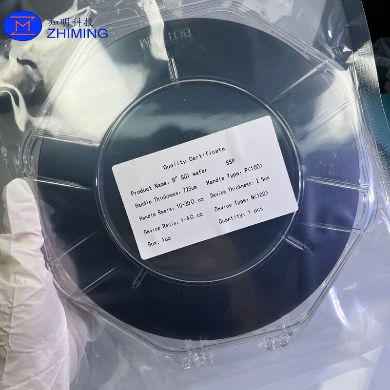
Created with Pixso. SOI Wafer:Lower parasitic capacitance stronger latch-up immunity improved radiation resistance

SOI Wafer:Lower parasitic capacitance stronger latch-up immunity improved radiation resistance

Brand Name: ZMSH
Model Number: SOI Wafer
MOQ: 25
Price: Fluctuates with market
Delivery Time: 2-4 weeks
Payment Terms: T/T
Detail Information
Place of Origin:
SHANGHAI,CHINA
Material:
Silicon Dioxide (SiO₂)/Silicon (Si)
Wafer Diameter:
Customized
Device Layer Thickness:
Customized
BOX Layer Thickness:
Customized
Crystal Orientation:
<100> / <110> / <111> / Customized
Conductivity Type:
N-Type / P-Type / Customized
Product Description

 Product Information

     
      SOI (Silicon-on-Insulator) is a “sandwich” structure wafer consisting of three layers: the top silicon layer, also known as the Top Si / Device Layer, is used to fabricate transistors; the middle layer is the Buried Oxide (BOX), which provides electrical isolation; and the bottom layer is the silicon support substrate (Handle/Substrate Wafer).

      Compared with conventional Bulk Si wafers, SOI wafers feature complete dielectric isolation, enabling lower parasitic capacitance and leakage current, stronger latch-up immunity, improved radiation resistance, and lower power consumption. As a result, SOI is a key substrate material for RF front-end devices, power devices, FD-SOI logic processes, photonics, MEMS, and other advanced semiconductor applications.
 

SOI Wafer:Lower parasitic capacitance stronger latch-up immunity improved radiation resistanceSOI Wafer:Lower parasitic capacitance stronger latch-up immunity improved radiation resistance         


Process Objectives

      The core objective of SOI wafer manufacturing is to obtain a single-crystal silicon thin film on top of an insulating layer, with precisely controlled thickness, crystal quality comparable to bulk silicon, and an ultra-smooth surface approaching atomic-level flatness.

Specifically, the process aims to:

      ① Precisely control the thickness of the device layer and BOX layer, with nanometer-level thickness uniformity. For FD-SOI, the top silicon layer typically requires a thickness uniformity on the order of ±0.5 nm.

      ② Maintain high single-crystal quality in the top silicon layer, with low dislocation density, long minority-carrier lifetime, and no residual lattice damage such as HDD.

      ③ Achieve high breakdown strength, low leakage current, and low interface-state density in the BOX layer, with an electric field strength on the order of >10 MV/cm.

      ④ Ensure a void-free bonding interface, without local delamination risks, while providing long-term reliability that meets device requirements.

      ⑤ Ensure that surface particles, metallic contamination, and surface roughness meet the cleanliness and quality requirements for IC-grade semiconductor applications.
                                                             SOI Wafer:Lower parasitic capacitance stronger latch-up immunity improved radiation resistance


Comparison of Mainstream SOI Manufacturing Routes


Technology Route Principle Key Features
Smart Cut™(Ion-Cut) Hydrogen ions are implanted into the silicon wafer to form a weakened layer. After wafer bonding, thermal annealing causes the implanted layer to split, forming the desired top silicon layer thickness. Mainstream industry technology, licensed under Soitec patents; provides precise thickness control, wafer reuse/recycling capability, and high production efficiency.
BESOI( Bonded and Etch-back SOI) High-dose oxygen ions are implanted into the silicon wafer, followed by ultra-high-temperature annealing to form a buried oxide layer (BOX) within the silicon. Relatively simple process, suitable for power devices and other applications requiring a thick top silicon layer >1 µm, but achieving high thickness uniformity becomes more difficult for ultra-thin top silicon layers.
SIMOX
(Separation by IMplanted OXygen)
High-dose oxygen ions are implanted into the silicon wafer, followed by ultra-high-temperature annealing to form a buried oxide layer (BOX) within the silicon. Provides good BOX uniformity, but requires a very high implantation dose (approximately 10¹⁸ cm⁻²), resulting in higher manufacturing costs, while the achievable BOX thickness is subject to limitations.
ELTRAN
(Epitaxial Layer Transfer)
A silicon epitaxial layer is grown on porous silicon and subsequently transferred through processes such as vapor-phase oxidation and layer separation. Provides an effective self-stopping layer separation mechanism, but has largely withdrawn from the mainstream SOI market.


Detailed Smart Cut™ Process Flow

Process Overview:
Incoming Silicon Wafer Inspection → RCA Cleaning → Thermal Oxidation (BOX) → Hydrogen Ion Implantation → Cleaning / Surface Activation → Wafer Bonding → Splitting Annealing → Dehydrogenation Annealing → Rough Grinding / Thinning → CMP Finishing → Sacrificial Oxidation + Chemical Polishing → Inspection & Classification → Final Cleaning & Packaging
SOI Wafer:Lower parasitic capacitance stronger latch-up immunity improved radiation resistanceSOI Wafer:Lower parasitic capacitance stronger latch-up immunity improved radiation resistance


Step 1 | Incoming Wafer Inspection & RCA Cleaning

Process Objective:To remove particles, organic contaminants, metal ions, and the native oxide layer from the silicon wafer surface, obtaining a clean and hydrophilic (hydroxyl-terminated) surface for subsequent oxidation and wafer bonding.

Main Process:
SC-1 (NH₄OH/H₂O₂/DI for particle and organic removal)
→ DHF (dilute HF for native oxide removal)
→ SC-2 (HCl/H₂O₂/DI for metallic contaminant removal)
→ Overflow rinsing + slow-rinse drying (SRD)

Production
Equipment:

Fully automated 8-inch/12-inch batch wet cleaning systems (Wet Bench), single-wafer cleaners such as SDI and TEL systems, megasonic-assisted cleaning systems, and SRD dryers.

Materials & Process Chemicals:
Electronic-grade NH₄OH, H₂O₂, HCl, and HF; ultrapure deionized water (DIW, resistivity 18.2 MΩ·cm); and high-purity N₂.                                     


                                             SOI Wafer:Lower parasitic capacitance stronger latch-up immunity improved radiation resistance

Step 2 | Thermal Oxidation for BOX Growth

Process Objective:

To grow a high-quality thermal oxide layer on the surface of the Seed/Donor Wafer, which serves as the buried oxide (BOX) layer of the final SOI wafer. The typical thickness ranges from 25 nm to 3 µm, depending on the application. For example, some RF devices commonly use a low-resistivity substrate combined with a relatively thick BOX layer.

The oxide density, interface-state characteristics, and thickness uniformity directly affect the electrical insulation and breakdown performance of the BOX layer.

Main Process:
A Dry-Wet-Dry thermal oxidation sequence can be used, typically at 1000–1150°C. For higher-specification products, extended dry oxidation may be employed to obtain a denser oxide layer and improved interface quality.

Production Equipment:
Vertical oxidation furnaces, horizontal diffusion furnaces, and RTP rapid thermal oxidation systems (RTO).

Materials & Process Gases:
High-purity O₂ (≥99.999%), H₂ for wet-oxidation generation with a combustion chamber, high-purity N₂/Ar for inert atmospheres, quartz furnace tubes, and SiC wafer boats.

                                                  SOI Wafer:Lower parasitic capacitance stronger latch-up immunity improved radiation resistance


Step 3 | Hydrogen Ion Implantation — Core of Smart Cut™

Process Objective:
      Hydrogen ions such as H⁺, or combined H₂⁺/He⁺ ions, are implanted through the oxide layer into the silicon at a controlled depth, forming a micro-cavity or weakened layer. This depth corresponds to the final thickness of the SOI device layer.
      Typical implantation energies range from 10–200 keV, with implantation doses of approximately 2×10¹⁶–8×10¹⁶ ions/cm². The implantation energy and dose influence the thickness of the transferred layer and the final surface quality.


Key Controls:

  • Within-wafer implantation uniformity: <1%
  • Wafer cooling to prevent undesirable thermal effects during implantation
  • Ion beam stability
  • Electrostatic beam scanning or wafer rotation at higher energies to improve implantation uniformity

Production Equipment:
      High-energy / high-current ion implanters.

Materials & Components:
      High-purity H₂ gas for dissociation and ionization, SiC/graphite shielding components, and Faraday cup assemblies.


                                                 SOI Wafer:Lower parasitic capacitance stronger latch-up immunity improved radiation resistance

Step 4 | Surface Cleaning & Plasma Activation
Process Objective:

      After ion implantation, the wafer surface is cleaned to remove contaminants. The implantation surface and the Handle Wafer surface are then plasma-activated, commonly using N₂/O₂/Ar plasma, to increase surface hydroxyl density and improve bonding capability, enabling sufficient initial bond strength at room temperature.

Production Equipment:
      Plasma activation and wafer bonding systems integrating an RF plasma chamber and bonding chamber, together with single-wafer cleaning systems.

Materials & Process Gases:
      High-purity N₂, O₂ and Ar process gases, DIW, and dedicated cleaning chemicals.

Step 5 | Wafer Bonding
Process Objective:
      The activated Seed/Donor Wafer, with the oxide/implanted surface facing downward, is aligned and brought into contact with the Handle Wafer under a controlled atmosphere. Van der Waals forces and hydrogen bonding enable room-temperature direct bonding (Direct Bonding / SDB). Macroscopic voids should be avoided at the bonding interface.

Key Controls:

  • Bonding alignment accuracy
  • Chamber vacuum level
  • Prevention of gas entrapment at the wafer edge
  • Bonding wavefront propagation from the center toward the edge
  • Initial bond strength

Production Equipment:
      Fully automated cluster-type wafer bonding systems.

Materials & Process Gases:
      High-purity N₂ and DIW.


                   SOI Wafer:Lower parasitic capacitance stronger latch-up immunity improved radiation resistanceSOI Wafer:Lower parasitic capacitance stronger latch-up immunity improved radiation resistance

Step 6 | Splitting Anneal & Dehydrogenation Anneal
 

Process Objective :

① Splitting Anneal:Typically performed at 400–600°C. The increasing hydrogen pressure within the implanted micro-cavities drives crack propagation, causing the Seed/Donor Wafer to split along the predefined weakened layer. The resulting split surface generally exhibits nanometer-scale roughness.

② Dehydrogenation Anneal:Typically performed at 900–1100°C to remove residual hydrogen from the top silicon layer while further strengthening the Si–O–Si bonding interface and increasing the overall bond strength.


Production Equipment:

Cluster annealing furnaces, vertical annealing furnaces, and RTP systems.


Materials & Process Gases:

High-purity N₂/Ar, with some processes using atmospheres containing trace O₂; quartz boats and furnace tubes.


Note:

The split donor wafer can be reused after subsequent polishing, which is one of the important cost advantages of the Smart Cut™ process over conventional BESOI.

                                                       SOI Wafer:Lower parasitic capacitance stronger latch-up immunity improved radiation resistance


Step 7 | Rough Thinning (BESOI Route) / Grinding
Process Objective:

      For Smart Cut™, the split surface of the top silicon layer generally retains nanometer-scale surface variations, so a light grinding step using a diamond grinding wheel is first performed to remove larger surface irregularities.

      For the BESOI route, the bonded top silicon layer is typically ground down from approximately 725 µm to the target thickness, which may range from several micrometers to several tens of micrometers, followed by wet etching using a suitable etch-stop layer for finer thickness control.

Production Equipment :

      Silicon wafer grinders; wet chemical thinning systems may also be used for the BESOI process.

Materials & Process Consumables:

      Diamond grinding wheels, grinding slurry, and etchants for etch-stop processing in the BESOI route.

Step 8 | CMP — Chemical Mechanical Polishing

Process Objective:

      CMP is used to further reduce the top silicon layer to the target thickness while reducing surface roughness to RMS < 0.15 nm, based on a 1 × 1 µm AFM scan, in order to meet global and local planarity requirements.

This step is one of the key processes for achieving excellent device-layer thickness uniformity.

Key Controls :

  1. Polishing rate and selectivity

  2. Real-time endpoint detection, such as eddy-current or optical thickness monitoring

  3. Polishing-pad condition management

  4. Post-CMP cleaning to prevent particle and metallic residues

                                                              SOI Wafer:Lower parasitic capacitance stronger latch-up immunity improved radiation resistance
     

Step 8 | CMP — Chemical Mechanical Polishing

Process Objective:

CMP is used to further reduce the top silicon layer to the target thickness while reducing surface roughness to RMS < 0.15 nm, based on a 1 × 1 µm AFM scan, in order to meet global and local planarity requirements.

This step is one of the key processes for achieving excellent device-layer thickness uniformity.

Key Controls :

  • Polishing rate and selectivity

  • Real-time endpoint detection, such as eddy-current or optical thickness monitoring

  • Polishing-pad condition management

  • Post-CMP cleaning to prevent particle and metallic residues


​Production Equipment:

CMP polishing systems + post-CMP scrubbers.

Materials & Consumables:

Alkaline silica-based slurry for silicon polishing, containing colloidal silica abrasives and KOH/amine-based pH modifiers; polyurethane polishing pads, DIW, and pad conditioners (disc dressers).

Step 9 | Sacrificial Oxidation & Final Chemical Polishing
Process Objective:

      A thin thermal oxide layer is grown on the CMP-finished top silicon, consuming approximately 10–20 nm of silicon. This transfers subsurface damage (SSD) and residual micro-defects introduced during CMP into the oxide layer, which is then removed using HF.

For selected products, an additional light Touch Polish / Final Polish may be applied to further improve the surface quality.

      This step helps reduce surface defect density and further improve the final wafer surface condition.

Production Equipment:
      Oxidation furnaces / RTO systems, batch HF etching and cleaning systems, and single-wafer final-polish CMP systems (optional).

Materials & Chemicals:
      High-purity O₂, BOE/HF buffered etchants, DIW, and N₂.


Step 10 | Inspection, Annealing & Final Packaging


Process Objective:

      Comprehensive dimensional, electrical, surface-quality and visual inspections are performed according to product specifications, followed by product classification such as Prime / Test / Control based on inspection results.

After final cleaning, the wafers are sealed and packaged under a controlled environment. Vacuum sealing or nitrogen-filled packaging may be used to minimize the risk of particle and environmental contamination during transportation and storage.


Production Equipment:

      Various wafer inspection and metrology systems, together with clean packaging lines including clean workstations and automated wafer-box loading equipment.


Packaging Materials:

      Wafer carriers such as FOSB, G1000 and open-type Empak systems, clean packaging bags, high-purity N₂, and labeling materials.


Metrology Items & Equipment
 

Measurement Item Typical Method / Equipment Typical Specification
Device Layer / BOX Thickness & Uniformity Reflectometry-based film thickness meters, ellipsometers (e.g. Onto, J.A. Woollam / JSV, etc.) Thin layers: ±0.5 nm; thick layers: ±1%–±5%
Surface Roughness Atomic Force Microscopy (AFM), 1×1 / 10×10 µm scan RMS < 0.15 nm (1 µm²)
Particles (LPD) Laser surface particle scanners (e.g. KLA SP series) Particles ≥0.09 µm: within several tens per wafer
HF Defects / Secco Defects HF etching + microscopic / automated defect inspection, assisted by laser microscopy HF Defect < 0.05~0.1 /cm²
Bonding Voids / Interface Defects Scanning Acoustic Microscopy (SAM/C-SAM), infrared (IR) inspection No detectable voids; detection limit typically at the mm scale depending on product specification
Metal Contamination Total Reflection X-ray Fluorescence (TXRF), VPD-ICP-MS, Surface Photovoltage (SPV) < Each element: <1×10¹⁰–5×10¹⁰ at/cm²
Crystal Defects (Dislocation / HDD / FPD) Wright/Jenkins etching + optical microscopy, XRD rocking curve EPD < 100 /cm², depending on product grade
(TTV/Bow/Warp/Flatness)
Geometry (TTV / Bow / Warp / Flatness)
Laser- or capacitance-based wafer geometry metrology Bow/Warp < 30–40 µm; TTV < 1–2 µm
Minority Carrier Lifetime (Handle / Device Layer) Microwave Photoconductivity Decay (µ-PCD) Depending on substrate specification; typically >100 µs for high-resistivity substrates
BOX Breakdown Voltage / Leakage C-V / I-V structure testing (destructive sampling) BOX breakdown electric field >5–10 MV/cm


                                                          SOI Wafer:Lower parasitic capacitance stronger latch-up immunity improved radiation resistance
 

Main Raw Materials & Process Consumables


Category Details Purity / Grade Requirements
Basic Materials Polished silicon wafers (Seed/Donor Wafer and Handle Wafer, including high-resistivity, low-resistivity and heavily doped grades) SEMI Prime Grade
Process Gases O₂, N₂, Ar, H₂, He (for ion implantation) ≥5N–6N electronic grade
Wet Chemicals NH₄OH, H₂O₂, HCl, HF/BOE, KOH/TMAH (for BESOI thinning) SEMI G1–G5 grade, depending on the process step
CMP Consumables Silicon polishing slurry (colloidal SiO₂ abrasives), polishing pads, and pad conditioners IC grade, low metallic contamination
Grinding Consumables Diamond grinding wheels (rough grinding), ceramic grinding wheels Grit size selected according to the process
Ultrapure Water / Others DIW (18.2 MΩ·cm), N₂ purge, clean packaging materials, quartz / SiC furnace components UPW grade / Class 1 purification


Manufacturing Environment Requirements
 

① <br>Cleanliness:CMP, cleaning, inspection and packaging should be performed in ISO Class 3–4 (Class 1–10) cleanrooms. Areas for oxidation, annealing and ion implantation should be maintained at ISO Class 5–6 or better.

② <br>Temperature & Humidity:Ambient temperature: 22±1°C; metrology rooms are recommended at 20±0.5°C for improved film-thickness measurement accuracy. Relative humidity: 40%–50%; the pre-bonding area is recommended at 45%±5% to maintain stable surface hydroxyl conditions.

③ <br>Vibration Control:Areas for CMP, optical film-thickness measurement and AFM should use isolated foundations or vibration-isolation measures and comply with the ISO VC vibration criteria specified by equipment manufacturers, minimizing measurement noise and polishing-related surface patterns.

④ <br>UPW & Chemicals:Ultrapure water (UPW) should have a resistivity of 18.2 MΩ·cm at 25°C and TOC <5 ppb. Electronic-grade chemicals should be controlled according to applicable SEMI standards and may be supplied through a centralized chemical management and supply system (CMS).

⑤ ESD 与交叉污染<br>ESD & Cross-Contamination Control:High-resistivity wafers are more susceptible to electrostatic effects and particle attraction; ionizers, grounding and other ESD-control measures are therefore required. Equipment, fixtures and consumables should be segregated between different doping specifications to prevent cross-contamination and resistivity drift.

                                               SOI Wafer:Lower parasitic capacitance stronger latch-up immunity improved radiation resistance


Conclusion
 

      SOI wafers are a classic example of “Material as Device,” where a silicon thin film with nanometer-level thickness control directly influences the performance limits of downstream semiconductor devices.

From RCA cleaning, which establishes a highly controlled and contamination-free starting surface, to hydrogen ion implantation, which precisely defines the splitting layer, and finally to CMP (Chemical Mechanical Polishing) and sacrificial oxidation, which create an ultra-smooth, low-defect surface, every stage represents a precise integration of materials, equipment, and metrology technologies.

As applications such as FD-SOI, RF front-end devices, silicon photonics, and high-voltage power devices continue to develop, SOI wafer manufacturing faces increasingly stringent requirements for device-layer thickness control, BOX performance, surface quality, and defect management, driving SOI technology toward ever-higher precision, lower defect levels, and improved reliability.

Related Products

                                                                 SOI Wafer:Lower parasitic capacitance stronger latch-up immunity improved radiation resistance
                                                              IC硅晶圆SSP / DSP表面处理<30/cm²,颗粒电阻率1~10欧姆


                                                                            SOI Wafer:Lower parasitic capacitance stronger latch-up immunity improved radiation resistance
                                                          8英寸硅碳晶圆碳化硅晶圆,底片假人,研究级,500微米,350微米.