logo
Good price  online

products details

Created with Pixso. Home Created with Pixso. Products Created with Pixso.
SiC Substrate
Created with Pixso. 6 Inch SiC As-Cut Wafer – Raw-Cut Unpolished Silicon Carbide Wafer

6 Inch SiC As-Cut Wafer – Raw-Cut Unpolished Silicon Carbide Wafer

Brand Name: ZMSH
MOQ: 25
Delivery Time: 2-4 weeks
Payment Terms: T/T
Detail Information
Place of Origin:
SHANGHAI,CHINA
Material:
Silicon Carbide (SiC)
Product Type:
As-Cut Wafer / Raw-Cut Wafer
Diameter:
6 Inch / 150 Mm
Crystal Polytype:
4H-SiC / 6H-SiC / Custom
Conductivity Type:
N-Type / Semi-Insulating / Custom
Orientation:
(0001) Or Customized
Thickness:
Customized
Product Description

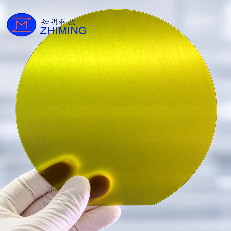
6 Inch SiC As-Cut Wafer – Raw-Cut Unpolished Silicon Carbide WaferOur 6 Inch SiC As-Cut Wafer is produced directly from high-quality silicon carbide crystal ingots through precision wire slicing. The wafer retains the original as-cut surface condition without subsequent grinding, lapping, polishing, or CMP processing.

Compared with polished SiC substrates, as-cut wafers provide a more cost-effective solution for customers who require raw silicon carbide wafers for downstream machining, thinning, grinding, polishing, equipment calibration, process development, or material testing.

The wafers can be supplied with customized thickness, crystal type, conductivity type, orientation, and surface condition according to customer requirements.


Key Features

  • 6-inch / 150 mm silicon carbide wafer

  • Raw-cut / as-cut surface

  • No CMP or final polishing

  • Suitable for grinding, lapping and polishing processes

  • Available in different SiC crystal types

  • Thickness can be customized

  • Suitable for equipment testing and process development

  • Lower cost compared with polished SiC substrates

  • Custom specifications available for R&D and industrial applications


Typical Specifications

Item Specification
Material Silicon Carbide (SiC)
Product Type As-Cut Wafer / Raw-Cut Wafer
Diameter 6 Inch / 150 mm
Crystal Polytype 4H-SiC / 6H-SiC / Custom
Conductivity Type N-Type / Semi-Insulating / Custom
Orientation (0001) or Customized
Thickness Customized
Surface As-Cut, Unpolished
Processing Wire Sliced
Edge Flat / Notch / Customized
Grade Research / Dummy / Test / Customized
Quantity Sample and Batch Orders Available

Final specifications should be confirmed according to application and customer requirements.


Surface Condition

6 Inch SiC As-Cut Wafer – Raw-Cut Unpolished Silicon Carbide WaferThe surface of the SiC wafer remains in the original condition after wire slicing and may show visible cutting marks or linear surface textures.

This type of wafer is normally supplied before:

  • Grinding

  • Lapping

  • Thinning

  • Mechanical polishing

  • CMP polishing

  • Surface finishing

For customers who need SSP, DSP or CMP polished SiC wafers, additional processing options are also available.


Applications

Grinding and Lapping Process Development

6-inch SiC as-cut wafers are suitable for evaluating grinding wheels, lapping plates, abrasives and machining parameters.

Polishing and CMP Testing

They can be used as starting wafers for developing mechanical polishing and chemical mechanical polishing processes.

Semiconductor Equipment Testing

Suitable for wafer handling, grinding, thinning, polishing and other semiconductor equipment testing.

Process Development

Used by universities, research institutes and semiconductor manufacturers for developing SiC wafer processing technologies.

Dummy and Test Wafers

As-cut SiC wafers can also be used as lower-cost test wafers when device-grade polished surfaces are not required.

Material Research

Suitable for research related to silicon carbide machining, surface treatment, crystal processing and material characterization.


Why Choose As-Cut SiC Wafers?

For applications where a polished device-grade surface is not necessary, as-cut wafers can significantly reduce material cost.

They are especially suitable for customers developing their own:

  • Wafer grinding processes

  • Wafer thinning processes

  • Surface polishing technology

  • CMP processes

  • Semiconductor equipment

  • SiC machining technology

The customer can perform subsequent processing according to their own process requirements.


Customization Available

We can provide customized SiC as-cut wafers according to your technical requirements, including:

  • Wafer diameter

  • Wafer thickness

  • Thickness tolerance

  • Crystal polytype

  • Conductivity type

  • Crystal orientation

  • Off-axis angle

  • Flat or notch configuration

  • Surface condition

  • Edge processing

  • Quantity

  • Additional grinding or polishing

For special test wafer requirements, please send us your drawing or specification sheet for evaluation.


Available Processing Options

In addition to as-cut SiC wafers, further processing can be provided upon request:

As-Cut → Grinding → Lapping → SSP → DSP → CMP

This allows customers to purchase SiC wafers at different processing stages depending on their production or R&D requirements.


Order Information

6 Inch SiC As-Cut Wafer – Raw-Cut Unpolished Silicon Carbide WaferWhen requesting a quotation, please provide the following information:

  1. Wafer diameter

  2. Required thickness

  3. Crystal polytype

  4. Conductivity type

  5. Crystal orientation

  6. Surface condition

  7. Flat or notch requirement

  8. Quantity

  9. Application

  10. Any special tolerance requirements

Samples and customized batch orders are available.

Contact us for technical evaluation, quotation and lead time.


Related Products

6 Inch SiC As-Cut Wafer – Raw-Cut Unpolished Silicon Carbide Wafer

6 inch N-type 6H Silicon Carbide Epitaxy Wafer with 350um Thickness for MEMS and UV Sensors