


Contact Us
Inquiry
If you have any questions, please contact us immediately and we will respond as soon as possible
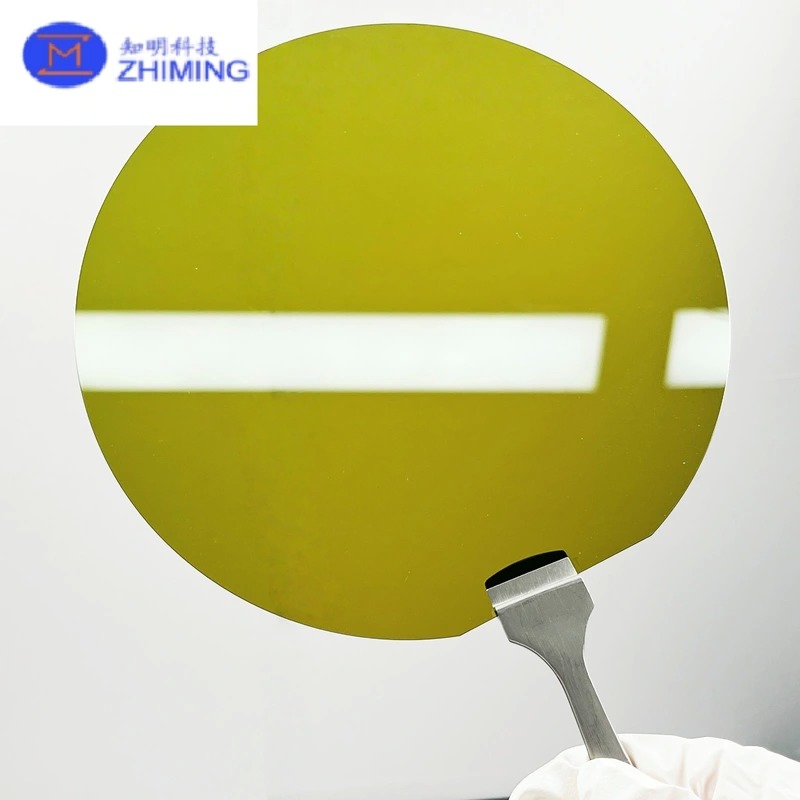
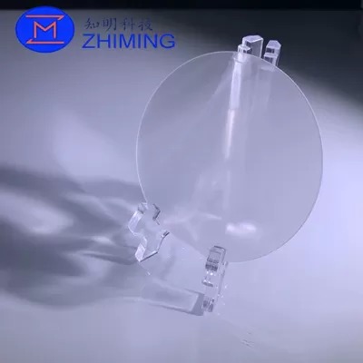
Products


Products