logo
Home ProductsGallium Nitride Wafer

10x10mm 10x15mm 001 Gallium oxide GaO substrate Mg doping Ga2O3 Gallium Nitride Wafer

I'm Online Chat Now

10x10mm 10x15mm 001 Gallium oxide GaO substrate Mg doping Ga2O3 Gallium Nitride Wafer

10x10mm 10x15mm 001 Gallium oxide GaO substrate Mg doping Ga2O3 Gallium Nitride Wafer
10x10mm 10x15mm 001 Gallium oxide GaO substrate Mg doping Ga2O3 Gallium Nitride Wafer 10x10mm 10x15mm 001 Gallium oxide GaO substrate Mg doping Ga2O3 Gallium Nitride Wafer 10x10mm 10x15mm 001 Gallium oxide GaO substrate Mg doping Ga2O3 Gallium Nitride Wafer

Large Image :  10x10mm 10x15mm 001 Gallium oxide GaO substrate Mg doping Ga2O3 Gallium Nitride Wafer

Product Details:
Place of Origin: china
Brand Name: zmsh
Certification: ROHS
Model Number: GaO substrates
Payment & Shipping Terms:
Minimum Order Quantity: 10pcs
Price: by case
Packaging Details: PET film in 100-grade cleaning room
Delivery Time: 1-4weeks
Supply Ability: 500pcs/month
Detailed Product Description
Industry: Semicondutor Wafer For Ld Or Led Application: Semiconductor Substrate, Led Chip, Optical Glass Window,device Substrates
Size: Customized Surface: Cmp/etched
Doped: Si-doped MOQ: 10PCS
Grade: Research Grade/dummy Grade
Highlight:

Gallium Oxide Ga2O3 Substrate

,

Single Crystal Ga2O3 Substrate

,

Ga2O3 Gallium Nitride Wafer

10x15mm 001 Gallium oxide GaO substrate Mg doping
 
10x10mm Gallium oxide substrate monocline structure
------------------------------------------------------------------------------------------------------------------------------

Specification detail
 
Orientation 100 100 100
Doping UID Mg Fe
electrical parameter
1×10¹⁷~3×1018cm-3
≥1010Ω·cm ≥1010Ω·cm
arcsec
≤150 ≤150 ≤150
dislocation density <1×105 cm-2 <1×105 cm-2 <1×105 cm-2


10x10mm 10x15mm 001 Gallium oxide GaO substrate Mg doping Ga2O3 Gallium Nitride Wafer 0


ABOUT OUR ZMKJ

     ZMKJ locates in the city of Shanghai, Which is the best city of China, and our factory is founded
in Wuxi city in 2014.We specialize in processing a varity of materials into wafers, substrates
and custiomized optical glass parts.components widely used in electronics, optics,
optoelectronics and many other fields. We also have been working closely with many domestic
and oversea universities, research institutions and companies, provide customized products
and services for their R&D projects.


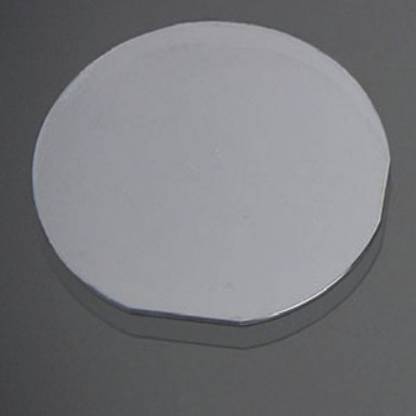
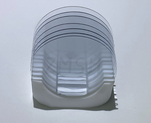
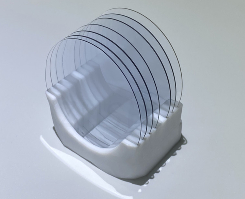
Related products:GaAs wafer
10x10mm 10x15mm 001 Gallium oxide GaO substrate Mg doping Ga2O3 Gallium Nitride Wafer 110x10mm 10x15mm 001 Gallium oxide GaO substrate Mg doping Ga2O3 Gallium Nitride Wafer 2
 
 
Packaging – Logistcs
Worldhawk concerns each details of the package , cleaning, anti-static , shock treatment .
According to the quantity and shape of the product , we will take a different packaging process!
 
FAQ –
Q: What you can supply logistics and cost?
(1) We accept DHL, Fedex, TNT, UPS, EMS, SF and  by FOB
 and pay condition of 50% deposit,50% before delivery.
 
Q: What's the delivery time?
For inventory: the delivery is 5 workdays after order.
For customized products: the delivery is 2 or 3 workweeks after order.
 

Q: What's the MOQ?
(1) For inventory, the MOQ is 5pcs.
(2) For customized products, the MOQ is 10pcs-30pcs.
Q: Do you have inspection report for material?
We can supply detail report for our products.


Contact Details
SHANGHAI FAMOUS TRADE CO.,LTD

Contact Person: Mr. Wang

Tel: +8615801942596

Send your inquiry directly to us (0 / 3000)