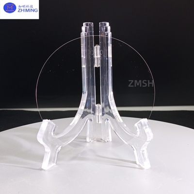
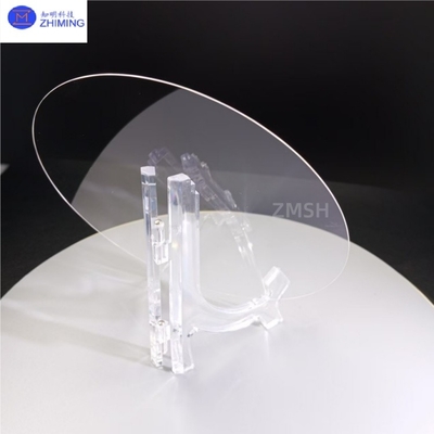
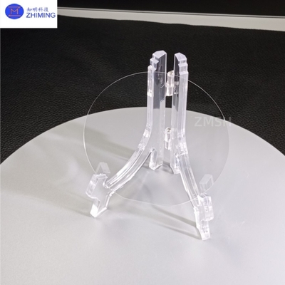
6inch Sapphire Wafer DSP Diameter 150mm Thickness 350μm For Power Electronics
The 6-inch sapphire wafer is a large-format optical-grade substrate fabricated from single-crystal aluminum oxide (α-Al₂O₃) via Edge-defined Film-fed Growth (EFG) or Kyropoulos (KY) methods, with standardized dimensions of 150mm±0.2mm diameter and customizable thickness (0.3-1.0mm). As a critical substrate for third-generation semiconductors, the 6-inch sapphire wafer combines high optical transmittance (>85% in visible spectrum), low lattice mismatch (13% with GaN), and exceptional mechanical stability, making it ideal for manufacturing high-brightness LEDs, Micro-LEDs, and power electronic devices. Its large-area format significantly enhances epitaxial production efficiency while reducing per-chip costs, driving advancements in optoelectronics and semiconductor industries.
Key Characteristics

1. 6inch sapphire wafer of superior Crystal Quality:
· Dislocation density <10³ cm⁻² with surface roughness Ra<0.3nm (C-plane polished), meeting atomic-level flatness requirements for GaN epitaxy.
· Crystal orientation accuracy ±0.1° (available in C-, R-, and A-plane orientations).
2. 6inch sapphire wafer of optical Performance:
· 85% transmittance in visible spectrum (400-800nm) and >80% in UV range (250-400nm), suitable for UV photonic devices.
· Customizable Double-Side Polished (DSP) or Patterned Sapphire Substrate (PSS) structures to enhance LED light extraction efficiency by >30%.
3. 6inch sapphire wafer of thermal/Mechanical Stability:
· Melting point 2040℃ with matched CTE (5.3×10⁻⁶/℃ to GaN), minimizing thermal stress cracks during epitaxy.
· Plasma-resistant for MOCVD/PECVD deposition processes.
4. 6inch sapphire wafer of large-Area Advantage:
· 50% more usable chip area per 6-inch wafer versus 4-inch equivalents, substantially reducing unit production costs.
Technical Parameters
| Property |
6inch |
| Diameter |
150±0.1mm |
| Thickness |
350±15um |
| 500 ± 15 um |
| 1000±15um |
| Roughness |
Ra ≤ 0.2nm |
| Warp |
≤ 15um |
| TTV |
≤ 10um |
| Scratch/Dig |
20/10 |
| Polish |
DSP (Double Side Polished); SSP(Single Side Polished) |
| Shape |
Round, Flat 16mm;OF length 22mm; OF Length 30/32.5mm; OF Length47.5mm; NOTCH; NOTCH; |
| Edge Form |
45°,C Shape |
| Material |
Sapphire crystal, Fused Quartz JGS1/JGS2; BF33, D263; EXG glass. |
| Remarks |
All specifications above can be customized upon your request |
Primary Applications

1. LED Manufacturing:
6inch sapphire wafer as the primary substrate for GaN epitaxy, 6-inch sapphire wafers enable high-yield production of high-brightness LEDs and Mini/Micro-LED display chips, supporting next-gen ultra-HD displays.
2. Power Electronics:
6inch sapphire wafer is used in GaN-on-sapphire HEMT devices for 5G base stations and EV power inverters requiring high-frequency/high-power operation.
3. Optical Components:
When precision-polished, 6inch sapphire wafer serves as extreme-environment windows (spacecraft) or UV sensor substrates with radiation resistance.
4. Semiconductor Equipment:
6inch sapphire wafer utilized as corrosion-resistant, high-insulation (resistivity >10¹⁴ Ω·cm) carrier plates for etching/ion implantation systems.

 Your message must be between 20-3,000 characters!
 Please check your E-mail!
  Your message must be between 20-3,000 characters!
 Please check your E-mail!


