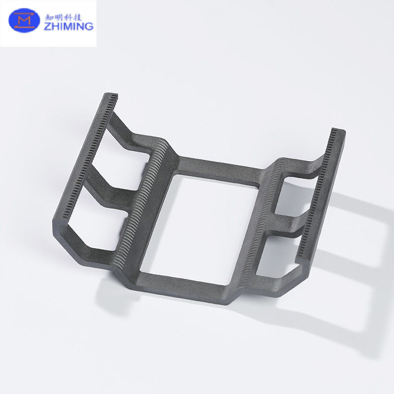
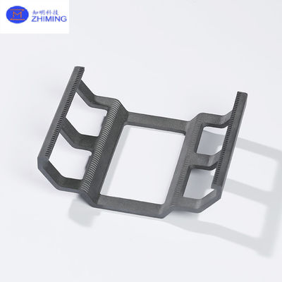
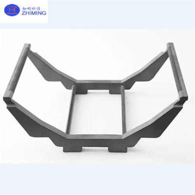
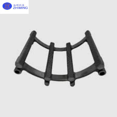
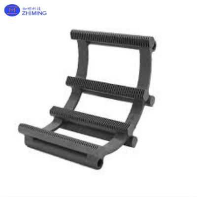
Customized SiC Ceramic Boat Carrier for Wafer Handling
The Customized Silicon Carbide (SiC) Ceramic Boat Carrier is a high-performance wafer handling solution designed for semiconductor, photovoltaic, and LED manufacturing processes. Engineered for high-temperature stability, chemical resistance, and ultra-low contamination, this carrier ensures safe and efficient wafer transport in demanding environments such as CVD, diffusion furnaces, and oxidation chambers.

Key Advantages of SiC Ceramic Boat
High Thermal Stability – Withstands temperatures up to 1,600°Cwithout deformation.
Chemical Inertness – Resists acids, alkalis, and plasma erosion, ensuring long-term durability.
Low Particle Generation – Minimizes contamination in EUV and advanced node fabrication.
Customizable Design – Tailored for wafer size, slot pitch, and handling requirements
Ideal for semiconductor fabs, MEMS production, and compound semiconductor processing
Specification
| Silicon Carbide Content | - | % | >99.5 |
| Average Grain Size | - | micron | 4-10 |
| Bulk Density | - | kg/dm^3 | >3.14 |
| Apparent Porosity | - | Vol % | <0.5 |
| Vickers Hardness | HV0.5 | Kg/mm^2 | 2800 |
| Modulus of Rupture (3 points) | 20°C | MPa | 450 |
| Compression Strength | 20°C | MPa | 3900 |
| Modulus of Elasticity | 20°C | GPa | 420 |
| Fracture Toughness | - | MPa/m^1/2 | 3.5 |
| Thermal Conductivity | 20°C | W(m*K) | 160 |
| Electrical Resistivity | 20°C | Ohm.cm | 10^6-10^8 |
| Coefficient of Thermal Expansion | a
(RT"800°C) | K^-1*10^-6 | 4.3 |
| Max. Application Temperature | Oxide Atmosphere | °C | 1600 |
| Max. Application Temperature | Inert Atmosphere | °C | 1950
|
Applications of SiC Ceramic Boat
1. Semiconductor Manufacturing
✔ Diffusion & Annealing Furnaces
- High-Temperature Stability – Withstands 1,600°C (oxidizing) / 1,950°C (inert) without deformation.
- Low Thermal Expansion (4.3×10⁻⁶/K) – Prevents wafer warpage in rapid thermal processing (RTP).
✔ CVD & Epitaxy (SiC/GaN Growth)
- Gas Corrosion Resistance – Inert to SiH₄, NH₃, HCl, and other aggressive precursors.
- Particle-Free Surface – Polished (Ra <0.2μm) for defect-free epitaxial deposition.
✔ Ion Implantation
- Radiation-Hardened – No degradation under high-energy ion bombardment.
2. Power Electronics (SiC/GaN Devices)
✔ SiC Wafer Processing
- CTE Matching (4.3×10⁻⁶/K) – Minimizes stress in 1,500°C+ epitaxial growth.
- High Thermal Conductivity (160 W/m·K) – Ensures uniform wafer heating.
✔ GaN-on-SiC Devices
- Non-Contaminating – No metal ion release vs. graphite boats.
3. Photovoltaic (Solar Cell) Production
✔ PERC & TOPCon Solar Cells
- POCl₃ Diffusion Resistance – Withstands phosphorus doping environments.
- Long Service Life – 5-10 years vs. 1-2 years for quartz boats.
✔ Thin-Film Solar (CIGS/CdTe)
- Corrosion Resistance – Stable in H₂Se, CdS deposition processes.
4. LED & Optoelectronics
✔ Mini/Micro-LED Epitaxy
- Precision Slot Design – Holds fragile 2"–6" wafers without edge chipping.
- Cleanroom-Compatible – Meets SEMI F57 particle standards.
5. Research & Specialty Applications
✔ High-Temp Material Synthesis
- Sintering Aids (e.g., B₄C, AlN) – Chemically inert in 2,000°C+ environments.
- Crystal Growth (e.g., Al₂O₃, ZnSe) – Non-reactive with molten materials.
FAQ
Q1: What wafer sizes are supported?
Standard: 150mm (6"), 200mm (8"), 300mm (12"). Customization available upon request.
Q2: What is the lead time for customized designs?
- Standard models: 4–6 weeks.
- Fully customized: 8–12 weeks (depending on complexity).

 Your message must be between 20-3,000 characters!