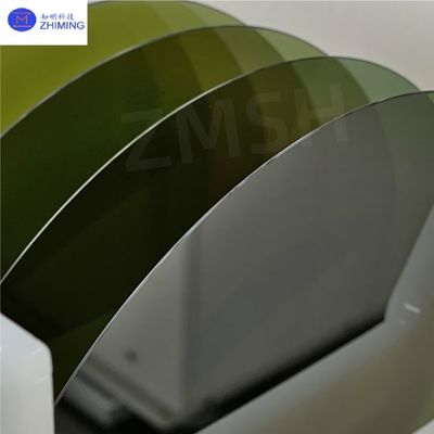
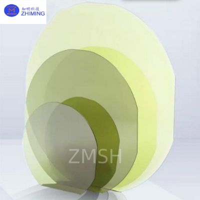
2inch 3inch 4inch 6inch SiC Epitaxial Wafers 4H-N Production Grade
Company Profile:
As a leading SiC (Silicon Carbide) epitaxial wafer supplier, ZMSH specialize in the production, processing, and global distribution of high-quality 4H-N-type conductive and MOS-grade epitaxial wafers in 2-inch (50.8mm), 3-inch (76.2mm), 4-inch (100mm), and 6-inch (150mm) diameters, with capabilities extending up to 12-inch (300mm) for future industry demands.
Our product portfolio includes:
· 4H-N-type & 6H-N-type conductive SiC substrates (for power devices)
· High-Purity Semi-Insulating (HPSI) & SEMI-standard wafers (for RF applications)
· 4H/6H-P-type & 3C-N-type SiC wafers (for specialized semiconductor needs)
· Custom doping, thickness, and surface finishes (CMP, epi-ready, etc.)
With advanced CVD epitaxial growth technology, strict quality control (ISO 9001), and full in-house processing capabilities, we serve automotive, power electronics, 5G, and aerospace industries worldwide.
Key parameters (2inch, 3inch, 4inch, 6inch 4H-N-Type Epi Wafers)
| Parameter |
Specifications |
| Crystal Structure |
4H-SiC (N-type) |
| Diameter |
2" / 3" / 4" / 6" |
| Epi Thickness |
5-50 µm (custom) |
| Doping Concentration |
1e15~1e19 cm⁻³ |
| Resistivity |
0.01–100 Ω·cm |
| Surface Roughness |
<0.2 nm (Ra) |
| Dislocation Density |
<1×10³ cm⁻² |
| TTV (Total Thickness Variation) |
<5 µm |
| Warpage |
<30 µm |
(All specs customizable – contact us for project-specific requirements.)
Key features of 4H-N SiC epitaxial wafers
1. Superior Electrical Performance
- SiC epitaxial wafers wide bandgap (3.2 eV) & high breakdown voltage (>2 MV/cm) for high-power devices
- SiC epitaxial wafers low on-resistance (R<sub>on</sub>) for efficient power conversion
2. Excellent Thermal Properties
- SiC epitaxial wafers high thermal conductivity (4.9 W/cm·K) for better heat dissipation
- SiC epitaxial wafers stable up to 600°C+, ideal for harsh environments
3. High-Quality Epitaxial Layer
- SiC epitaxial wafers low defect density (<1×10³ cm⁻²) for reliable device performance
- Uniform thickness (±2%) and doping control (±5%) for consistency
4. Multiple Wafer Grades Available
- Conductive Grade (for diodes, MOSFETs)
- MOSFET Grade (ultra-low defects for high-performance transistors)
Primary applications of 4H-N SiC epitaxial wafers

1. Electric Vehicles (EVs) & Fast Charging
- SiC MOSFETs & Schottky diodes for inverters and OBCs (higher efficiency than Si)
2. Renewable Energy & Industrial Power
- Solar inverters, wind turbines, and smart grids (lower energy loss)
3. 5G & RF Communications
- GaN-on-SiC RF devices for 5G base stations (high-frequency operation)
4. Aerospace & Defense
- SiC epitaxial wafers can be used for Radar, satellite comms, and high-voltage systems (extreme environment stability)
5. Consumer & Industrial Electronics
- SiC epitaxial wafers can be used for high-efficiency PSUs, motor drives, and UPS systems
ZMSH's Services of 4H-N SiC epitaxial wafers
1. Full-Cycle Manufacturing & Customization
· SiC substrate production (2" to 12")
· Epitaxial growth (CVD) with controlled doping (N/P-type)
· Wafer processing (lapping, polishing, laser marking, dicing)
2. Testing & Certification
· XRD (crystallinity), AFM (surface roughness), Hall effect (carrier mobility)
· Defect inspection (etch pit density, micropipes <1/cm²)
3. Global Supply Chain Support
· Fast prototyping & bulk order fulfillment
· Technical consulting for SiC device design
Why Choose Us?
✔ Vertical integration (substrate → epitaxy → finished wafer)
✔ High yield & competitive pricing
✔ R&D support for next-gen SiC devices
✔ Fast lead times & global logistics
(For datasheets, samples, or quotes – reach out today!)
FAQ of 4H-N SiC epitaxial wafers
1. Q: What are the key differences between 2-inch, 4-inch and 6-inch SiC epitaxial wafers?
A: The main differences are in production scalability (6" enables higher volume) and cost-per-chip (larger wafers reduce device costs by ~30%).
2. Q: Why choose 4H-SiC over silicon for power devices?
A: 4H-SiC offers 10x higher breakdown voltage and 3x better thermal conductivity than silicon, enabling smaller, more efficient power systems.
Tags: #2inch 3inch 4inch 6inch, #SiC Epitaxial Wafers, #Silicon Carbide#4H-N, #Conductive, #Production Grade, #MOS Grade

 Your message must be between 20-3,000 characters!